Intelligence is not added on, but arises directly from structure.
AI Acceleration Redefined
BREAK THE MEMORY WALL
LOW LATENCY
LOW ENERGY CONSUMPTION
SCALABILITY
Accelerating Critical AI Workloads
Data‑center AI offload for high‑throughput inference
Delivering high computing density to hyper-scaler server architectures, maximizing throughput per rack while reducing electrical footprints and eliminating thermal bottlenecks.

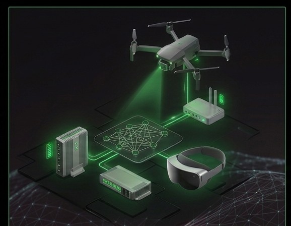
Edge AI for always‑on, low‑power devices
Empowering mobile hardware, sensor arrays, and remote gateways with smart models operating comfortably within constrained battery budgets.
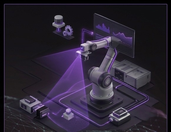
AI robotics for ultra‑low‑latency perception and control
Providing light-speed tactile reflexes and spatial sensory translation for high-speed robotic limbs, automated manufacturing, and autonomous drones.
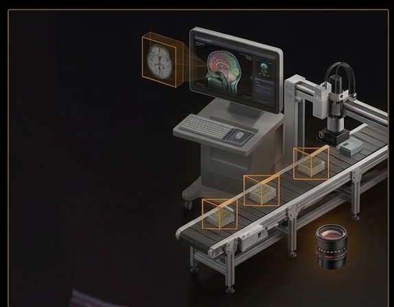
Medical imaging and industrial automation for fast, on‑device intelligence
Powering high-resolution diagnostic image pipelines and instantaneous automated optical inspections directly on the machine layer without cloud roundtrips.
Chip-scale photonic neural networks combining in-memory computing, one-shot inference, ~400M params/mm² computing density, and foundry-compatible manufacturing
The power of Photonic Neural Network(PNN)
Every OptoSwift chip is designed computationally before fabrication on silicon photonics processes. OptoSwift replaces your slow, power‑hungry dense layers with a PNN-based AI core, unlocking ultra‑low‑latency, ultra‑efficient inference while keeping model performance intact.
Weights are encoded in nanophotonic structures; the neural transformation happens in one optical pass as light propagates through the chip.
Read the paper (Nature Communications)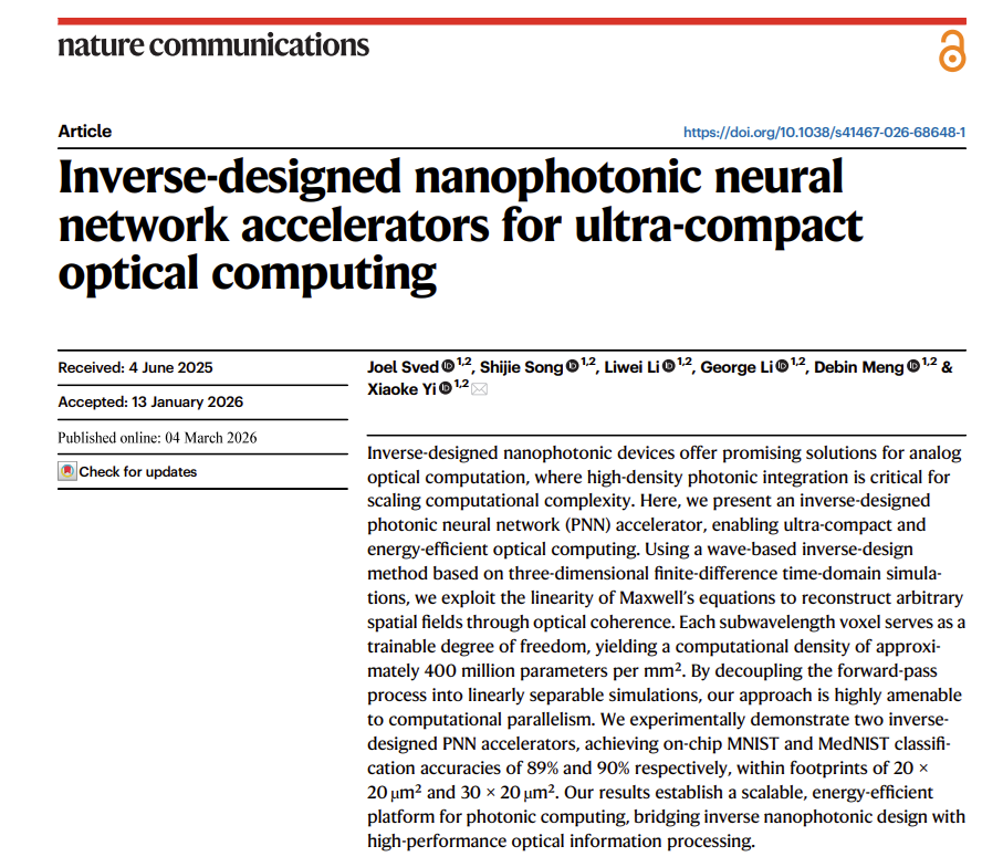
Photonic AI chips designed for the next era of energy‑efficient, low‑latency intelligence
We operate standard manufacturing and foundry processes to ensure extreme reliability. Let's collaborate to unlock optical performance benchmarks.
The world has taken notice
"This research performs neural computation using light, enabling faster, more energy-efficient and ultra-compact AI accelerators."
ABOUT OPTOSWIFT
A proven photonic AI team combining scientific leadership and semiconductor industry experience. Together, we bring the technical expertise, strategic partnerships and commercial insight needed to translate photonic innovation into practical AI computing solutions.
Leadership

Professor, University of Sydney. Fellow of Optica. Fellow of the Royal Society NSW. Australian Research Council QEII Fellow. Engineering Australia Most Innovative Engineer Award. Senior author, Nature Communications 2026. Co-inventor on 17 foreground IP assets. She leads the vision, strategy, and technological direction of OptoSwift.

B.E. (First Class Honours), PhD candidate (final year), University of Sydney. 1st author, Nature Communications 2026. RSNSW Bicentennial Scholar & Defence Innovation Network Scholar. John Pether Memorial Prize. Dalyell Scholar. Foundries MPW tape outs. Co-inventor on one foreground IP asset.

Postdoctoral Research Associate, University of Sydney. Harvard visiting scholar. 2nd author, Nature Communications 2026. 7+ years of cleanroom expertise and 10+ years' experience in photonic systems and MPW tape-out experience. Co-inventor on four foreground IP assets.

Founder and former CEO of X-Celeprint, with extensive experience in semiconductor and photonics commercialisation. Previously Senior Director of Business Development at Semprius, responsible for micro-transfer printing technology licensing, and led global support and commercial development of OLED polymers at Dow Chemical.
Advisors


University of Sydney Spin-out
How can we help you?
Submit your question or business inquiry directly. Our technical support and corporate relations desk typically responds in under 12 hours.
Office Address
Suite 20.01, Level 20, 133 Castlereagh Street, Sydney NSW 2000, Australia
Enquiries
info@optoswift.com